Example of IEEE Transactions on Electron Devices format
Recent searches

Example of IEEE Transactions on Electron Devices format Example of IEEE Transactions on Electron Devices format Example of IEEE Transactions on Electron Devices format Example of IEEE Transactions on Electron Devices format Example of IEEE Transactions on Electron Devices format Example of IEEE Transactions on Electron Devices format Example of IEEE Transactions on Electron Devices format
Sample paper formatted on SciSpace - SciSpace
This content is only for preview purposes. The original open access content can be found here.
Look Inside
Example of IEEE Transactions on Electron Devices format Example of IEEE Transactions on Electron Devices format Example of IEEE Transactions on Electron Devices format Example of IEEE Transactions on Electron Devices format Example of IEEE Transactions on Electron Devices format Example of IEEE Transactions on Electron Devices format Example of IEEE Transactions on Electron Devices format
Sample paper formatted on SciSpace - SciSpace
This content is only for preview purposes. The original open access content can be found here.
open access Open Access

IEEE Transactions on Electron Devices — Template for authors

Publisher: IEEE
Categories Rank Trend in last 3 yrs
Electrical and Electronic Engineering #146 of 693 down down by 35 ranks
Electronic, Optical and Magnetic Materials #58 of 246 down down by 13 ranks
journal-quality-icon Journal quality:
High
calendar-icon Last 4 years overview: 3236 Published Papers | 17905 Citations
indexed-in-icon Indexed in: Scopus
last-updated-icon Last updated: 16/06/2020
Related journals
Insights
General info
Top papers
Popular templates
Get started guide
Why choose from SciSpace
FAQ

Related Journals

open access Open Access

IEEE

Quality:  
High
CiteRatio: 5.5
SJR: 0.81
SNIP: 1.008
open access Open Access
recommended Recommended

Springer

Quality:  
High
CiteRatio: 15.9
SJR: 3.473
SNIP: 2.052
open access Open Access

IEEE

Quality:  
High
CiteRatio: 4.4
SJR: 0.732
SNIP: 1.305

Journal Performance & Insights

CiteRatio

SCImago Journal Rank (SJR)

Source Normalized Impact per Paper (SNIP)

A measure of average citations received per peer-reviewed paper published in the journal.

Measures weighted citations received by the journal. Citation weighting depends on the categories and prestige of the citing journal.

Measures actual citations received relative to citations expected for the journal's category.

5.5

4% from 2019

CiteRatio for IEEE Transactions on Electron Devices from 2016 - 2020
Year Value
2020 5.5
2019 5.3
2018 5.0
2017 4.7
2016 5.2
graph view Graph view
table view Table view

0.828

6% from 2019

SJR for IEEE Transactions on Electron Devices from 2016 - 2020
Year Value
2020 0.828
2019 0.879
2018 0.853
2017 0.839
2016 1.009
graph view Graph view
table view Table view

1.544

3% from 2019

SNIP for IEEE Transactions on Electron Devices from 2016 - 2020
Year Value
2020 1.544
2019 1.505
2018 1.453
2017 1.485
2016 1.67
graph view Graph view
table view Table view

insights Insights

  • CiteRatio of this journal has increased by 4% in last years.
  • This journal’s CiteRatio is in the top 10 percentile category.

insights Insights

  • SJR of this journal has decreased by 6% in last years.
  • This journal’s SJR is in the top 10 percentile category.

insights Insights

  • SNIP of this journal has increased by 3% in last years.
  • This journal’s SNIP is in the top 10 percentile category.

IEEE Transactions on Electron Devices

Guideline source: View

All company, product and service names used in this website are for identification purposes only. All product names, trademarks and registered trademarks are property of their respective owners.

Use of these names, trademarks and brands does not imply endorsement or affiliation. Disclaimer Notice

IEEE

IEEE Transactions on Electron Devices

IEEE Transactions on Electron Devices comprises original and significant contributions relating to the theory, design, performance and reliability of electron devices, including optoelectronic devices, nanoscale devices, solid-state devices, integrated electronic devices, ener...... Read More

Engineering

i
Last updated on
16 Jun 2020
i
ISSN
0018-9383
i
Impact Factor
High - 1.959
i
Open Access
No
i
Sherpa RoMEO Archiving Policy
Green faq
i
Plagiarism Check
Available via Turnitin
i
Endnote Style
Download Available
i
Bibliography Name
IEEEtran
i
Citation Type
Numbered
[25]
i
Bibliography Example
C. W. J. Beenakker, “Specular andreev reflection in graphene,” Phys. Rev. Lett., vol. 97, no. 6, p.

Top papers written in this journal

Journal Article DOI: 10.1109/T-ED.1969.16566
Large-signal analysis of a silicon Read diode oscillator
D.L. Scharfetter1, H.K. Gummel1

Abstract:

This paper presents theoretical calculations of the large-signal admittance and efficiency achievable in a silicon p-n-v-ns Read IMPATT diode. A simplified theory is employed to obtain a starting design. This design is then modified to achieve higher efficiency operation as specific device limitations are reached in large-sig... This paper presents theoretical calculations of the large-signal admittance and efficiency achievable in a silicon p-n-v-ns Read IMPATT diode. A simplified theory is employed to obtain a starting design. This design is then modified to achieve higher efficiency operation as specific device limitations are reached in large-signal (computer) operation. Self-consistent numerical solutions are obtained for equations describing carrier transport, carrier generation, and space-charge balance. The solutions describe the evolution in time of the diode and its associated resonant circuit. Detailed solutions are presented of the hole and electron concentrations, electric field, and terminal current and voltage at various points in time during a cycle of oscillation. Large-signal values of the diode's negative conductance, susceptance, average voltage, and power-generating efficiency are presented as a function of oscillation amplitude for a fixed average current density. For the structure studied, the largest microwave power-generating efficiency (18 percent at 9.6 GHz) has been obtained at a current density of 200 A/cm2, but efficiencies near 10 percent were obtained over a range of current density from 100 to 1000 A/cm2. read more read less

Topics:

IMPATT diode (62%)62% related to the paper, Susceptance (57%)57% related to the paper, Diode (56%)56% related to the paper, Voltage (54%)54% related to the paper, Current density (53%)53% related to the paper
2,042 Citations
Journal Article DOI: 10.1109/16.887014
FinFET-a self-aligned double-gate MOSFET scalable to 20 nm

Abstract:

MOSFETs with gate length down to 17 nm are reported To suppress the short channel effect, a novel self-aligned double-gate MOSFET, FinFET, is proposed By using boron-doped Si/sub 04/Ge/sub 06/ as a gate material, the desired threshold voltage was achieved for the ultrathin body device The quasiplanar nature of this new varian... MOSFETs with gate length down to 17 nm are reported To suppress the short channel effect, a novel self-aligned double-gate MOSFET, FinFET, is proposed By using boron-doped Si/sub 04/Ge/sub 06/ as a gate material, the desired threshold voltage was achieved for the ultrathin body device The quasiplanar nature of this new variant of the vertical double-gate MOSFETs can be fabricated relatively easily using the conventional planar MOSFET process technologies read more read less

Topics:

Short-channel effect (64%)64% related to the paper, Channel length modulation (61%)61% related to the paper, MOSFET (57%)57% related to the paper, Threshold voltage (52%)52% related to the paper
1,668 Citations
Journal Article DOI: 10.1109/T-ED.1979.19791
A gas chromatographic air analyzer fabricated on a silicon wafer
S. C. Terry1, J. H. Jerman1, J.B. Angell1

Abstract:

A miniature gas analysis system has been built based on the principles of gas chromatography (GC). The major components are fabricated in silicon using photolithography and chemical etching techniques, which allows size reductions of nearly three orders of magnitude compared to conventional laboratory instruments. The chromat... A miniature gas analysis system has been built based on the principles of gas chromatography (GC). The major components are fabricated in silicon using photolithography and chemical etching techniques, which allows size reductions of nearly three orders of magnitude compared to conventional laboratory instruments. The chromatography system consists of a sample injection valve and a 1.5-m-long separating capillary column, which are fabricated on a substrate silicon wafer. The output thermal conductivity detector is separately batch fabricated and integrably mounted on the substrate wafer. The theory of gas chromatography has been used to optimize the performance of the sensor so that separations of gaseous hydrocarbon mixtures are performed in less than 10 s. The system is expected to find application in the areas of portable ambient air quality monitors, implanted biological experiments, and planetary probes. read more read less

Topics:

Etching (microfabrication) (58%)58% related to the paper, Wafer (57%)57% related to the paper, Gas chromatography ion detector (56%)56% related to the paper, Thermal conductivity detector (55%)55% related to the paper, Silicon (51%)51% related to the paper
1,414 Citations
Journal Article DOI: 10.1109/16.337449
On the universality of inversion layer mobility in Si MOSFET's: Part I-effects of substrate impurity concentration
Shinichi Takagi1, A. Toriumi2, M. Iwase2, H. Tango2

Abstract:

This paper reports the studies of the inversion layer mobility in n- and p-channel Si MOSFET's with a wide range of substrate impurity concentrations (10/sup 15/ to 10/sup 18/ cm/sup -3/). The validity and limitations of the universal relationship between the inversion layer mobility and the effective normal field (E/sub eff/... This paper reports the studies of the inversion layer mobility in n- and p-channel Si MOSFET's with a wide range of substrate impurity concentrations (10/sup 15/ to 10/sup 18/ cm/sup -3/). The validity and limitations of the universal relationship between the inversion layer mobility and the effective normal field (E/sub eff/) are examined. It is found that the universality of both the electron and hole mobilities does hold up to 10/sup 18/ cm/sup -3/. The E/sub eff/ dependences of the universal curves are observed to differ between electrons and holes, particularly at lower temperatures. This result means a different influence of surface roughness scattering on the electron and hole transports. On substrates with higher impurity concentrations, the electron and hole mobilities significantly deviate from the universal curves at lower surface carrier concentrations because of Coulomb scattering by the substrate impurity. Also, the deviation caused by the charged centers at the Si/SiO/sub 2/ interface is observed in the mobility of MOSFET's degraded by Fowler-Nordheim electron injection. > read more read less

Topics:

Electron mobility (60%)60% related to the paper
View PDF
1,389 Citations
Journal Article DOI: 10.1109/16.906451
The impact of surface states on the DC and RF characteristics of AlGaN/GaN HFETs
Ramakrishna Vetury1, N.-Q. Zhang1, Stacia Keller1, Umesh K. Mishra1

Abstract:

GaN based HFETs are of tremendous interest in applications requiring high power at microwave frequencies. Although excellent current-voltage (I-V) characteristics and record high output power densities at microwave frequencies have been achieved, the origin of the 2DEG and the factors limiting the output power and reliability... GaN based HFETs are of tremendous interest in applications requiring high power at microwave frequencies. Although excellent current-voltage (I-V) characteristics and record high output power densities at microwave frequencies have been achieved, the origin of the 2DEG and the factors limiting the output power and reliability of the devices under high power operation remain uncertain. Drain current collapse has been the major obstacle in the development of reliable high power devices. We show that the cause of current collapse is a charging up of a second virtual gate, physically located in the gate drain access region. Due to the large bias voltages present on the device during a microwave power measurement, surface states in the vicinity of the gate trap electrons, thus acting as a negatively charged virtual gate. The maximum current available from a device during a microwave power measurement is limited by the discharging of this virtual gate. Passivated devices located adjacent to unpassivated devices on the same wafer show almost no current collapse, thus demonstrating that proper surface passivation prevents the formation of the virtual gate. The possible mechanisms by which a surface passivant reduces current collapse and the factors affecting reliability and stability of such a passivant are discussed. read more read less

Topics:

Power semiconductor device (56%)56% related to the paper
1,334 Citations
Author Pic

SciSpace is a very innovative solution to the formatting problem and existing providers, such as Mendeley or Word did not really evolve in recent years.

- Andreas Frutiger, Researcher, ETH Zurich, Institute for Biomedical Engineering

Get MS-Word and LaTeX output to any Journal within seconds
1
Choose a template
Select a template from a library of 40,000+ templates
2
Import a MS-Word file or start fresh
It takes only few seconds to import
3
View and edit your final output
SciSpace will automatically format your output to meet journal guidelines
4
Submit directly or Download
Submit to journal directly or Download in PDF, MS Word or LaTeX

(Before submission check for plagiarism via Turnitin)

clock Less than 3 minutes

What to expect from SciSpace?

Speed and accuracy over MS Word

''

With SciSpace, you do not need a word template for IEEE Transactions on Electron Devices.

It automatically formats your research paper to IEEE formatting guidelines and citation style.

You can download a submission ready research paper in pdf, LaTeX and docx formats.

Time comparison

Time taken to format a paper and Compliance with guidelines

Plagiarism Reports via Turnitin

SciSpace has partnered with Turnitin, the leading provider of Plagiarism Check software.

Using this service, researchers can compare submissions against more than 170 million scholarly articles, a database of 70+ billion current and archived web pages. How Turnitin Integration works?

Turnitin Stats
Publisher Logos

Freedom from formatting guidelines

One editor, 100K journal formats – world's largest collection of journal templates

With such a huge verified library, what you need is already there.
publisher-logos

Easy support from all your favorite tools

IEEE Transactions on Electron Devices format uses IEEEtran citation style.

Automatically format and order your citations and bibliography in a click.

SciSpace allows imports from all reference managers like Mendeley, Zotero, Endnote, Google Scholar etc.

Frequently asked questions

1. Can I write IEEE Transactions on Electron Devices in LaTeX?

Absolutely not! Our tool has been designed to help you focus on writing. You can write your entire paper as per the IEEE Transactions on Electron Devices guidelines and auto format it.

2. Do you follow the IEEE Transactions on Electron Devices guidelines?

Yes, the template is compliant with the IEEE Transactions on Electron Devices guidelines. Our experts at SciSpace ensure that. If there are any changes to the journal's guidelines, we'll change our algorithm accordingly.

3. Can I cite my article in multiple styles in IEEE Transactions on Electron Devices?

Of course! We support all the top citation styles, such as APA style, MLA style, Vancouver style, Harvard style, and Chicago style. For example, when you write your paper and hit autoformat, our system will automatically update your article as per the IEEE Transactions on Electron Devices citation style.

4. Can I use the IEEE Transactions on Electron Devices templates for free?

Sign up for our free trial, and you'll be able to use all our features for seven days. You'll see how helpful they are and how inexpensive they are compared to other options, Especially for IEEE Transactions on Electron Devices.

5. Can I use a manuscript in IEEE Transactions on Electron Devices that I have written in MS Word?

Yes. You can choose the right template, copy-paste the contents from the word document, and click on auto-format. Once you're done, you'll have a publish-ready paper IEEE Transactions on Electron Devices that you can download at the end.

6. How long does it usually take you to format my papers in IEEE Transactions on Electron Devices?

It only takes a matter of seconds to edit your manuscript. Besides that, our intuitive editor saves you from writing and formatting it in IEEE Transactions on Electron Devices.

7. Where can I find the template for the IEEE Transactions on Electron Devices?

It is possible to find the Word template for any journal on Google. However, why use a template when you can write your entire manuscript on SciSpace , auto format it as per IEEE Transactions on Electron Devices's guidelines and download the same in Word, PDF and LaTeX formats? Give us a try!.

8. Can I reformat my paper to fit the IEEE Transactions on Electron Devices's guidelines?

Of course! You can do this using our intuitive editor. It's very easy. If you need help, our support team is always ready to assist you.

9. IEEE Transactions on Electron Devices an online tool or is there a desktop version?

SciSpace's IEEE Transactions on Electron Devices is currently available as an online tool. We're developing a desktop version, too. You can request (or upvote) any features that you think would be helpful for you and other researchers in the "feature request" section of your account once you've signed up with us.

10. I cannot find my template in your gallery. Can you create it for me like IEEE Transactions on Electron Devices?

Sure. You can request any template and we'll have it setup within a few days. You can find the request box in Journal Gallery on the right side bar under the heading, "Couldn't find the format you were looking for like IEEE Transactions on Electron Devices?”

11. What is the output that I would get after using IEEE Transactions on Electron Devices?

After writing your paper autoformatting in IEEE Transactions on Electron Devices, you can download it in multiple formats, viz., PDF, Docx, and LaTeX.

12. Is IEEE Transactions on Electron Devices's impact factor high enough that I should try publishing my article there?

To be honest, the answer is no. The impact factor is one of the many elements that determine the quality of a journal. Few of these factors include review board, rejection rates, frequency of inclusion in indexes, and Eigenfactor. You need to assess all these factors before you make your final call.

13. What is Sherpa RoMEO Archiving Policy for IEEE Transactions on Electron Devices?

SHERPA/RoMEO Database

We extracted this data from Sherpa Romeo to help researchers understand the access level of this journal in accordance with the Sherpa Romeo Archiving Policy for IEEE Transactions on Electron Devices. The table below indicates the level of access a journal has as per Sherpa Romeo's archiving policy.

RoMEO Colour Archiving policy
Green Can archive pre-print and post-print or publisher's version/PDF
Blue Can archive post-print (ie final draft post-refereeing) or publisher's version/PDF
Yellow Can archive pre-print (ie pre-refereeing)
White Archiving not formally supported
FYI:
  1. Pre-prints as being the version of the paper before peer review and
  2. Post-prints as being the version of the paper after peer-review, with revisions having been made.

14. What are the most common citation types In IEEE Transactions on Electron Devices?

The 5 most common citation types in order of usage for IEEE Transactions on Electron Devices are:.

S. No. Citation Style Type
1. Author Year
2. Numbered
3. Numbered (Superscripted)
4. Author Year (Cited Pages)
5. Footnote

15. How do I submit my article to the IEEE Transactions on Electron Devices?

It is possible to find the Word template for any journal on Google. However, why use a template when you can write your entire manuscript on SciSpace , auto format it as per IEEE Transactions on Electron Devices's guidelines and download the same in Word, PDF and LaTeX formats? Give us a try!.

16. Can I download IEEE Transactions on Electron Devices in Endnote format?

Yes, SciSpace provides this functionality. After signing up, you would need to import your existing references from Word or Bib file to SciSpace. Then SciSpace would allow you to download your references in IEEE Transactions on Electron Devices Endnote style according to Elsevier guidelines.

Fast and reliable,
built for complaince.

Instant formatting to 100% publisher guidelines on - SciSpace.
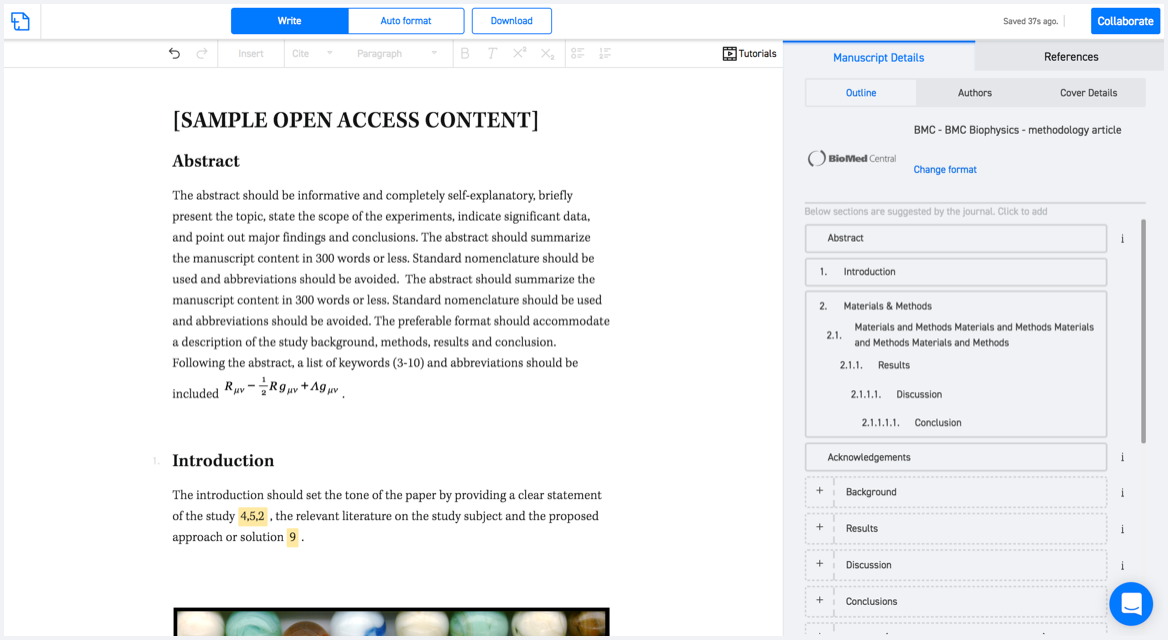
Available only on desktops 🖥

No word template required

Typset automatically formats your research paper to IEEE Transactions on Electron Devices formatting guidelines and citation style.
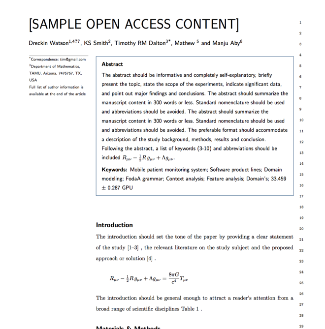
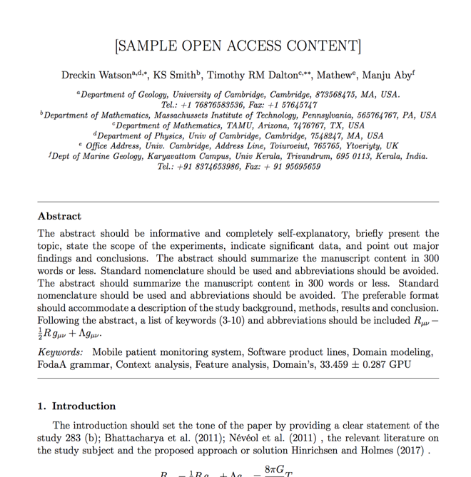
Verifed journal formats

One editor, 100K journal formats.
With the largest collection of verified journal formats, what you need is already there.

Trusted by academicians

I spent hours with MS word for reformatting. It was frustrating - plain and simple. With SciSpace, I can draft my manuscripts and once it is finished I can just submit. In case, I have to submit to another journal it is really just a button click instead of an afternoon of reformatting.

Andreas Frutiger
Researcher & Ex MS Word user
Use this template